What's Inside: UHF/SHF Amplifier Modules
In an effort to be prepared for figuring out how to work an integrated microwave SDR, I picked up three amplifier modules for 900, 1300, and 2400 MHz. They're all from the same eBay seller and presumably the same factory with matching enclosures, labeling, and design techniques.
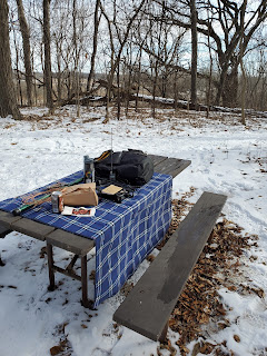
 |
| Lineup of the three amplifier modules (labeled 2.4G 10W, 1250, and 915) with the heatsink planned for future use. |
In descending frequency, let's get started with the 2.4 GHz module!
 |
| Initial lid removed from the 2.4 GHz module |
Taking the top off reveals a three-stage amplifier module and a bit of thermal paste running back up the thermal vias that didn't get filled with solder around the final PA. The bias network is all positive with a resistor dropper array into a linear regulator followed by a voltage divider for the final.
 |
| Focus on input stage of 2.4 GHz module |
The input two stages are wideband MMICs biased from the 9 V linear rail. With this closer look, here's the device chain:
- SBB4089Z (50MHz to 6000MHz Cascadable Amplifier, gain 15 dB, P1dB 19 dBm)
- AH102A-G (350 to 3000 MHz High Linearity Amplifier, gain 14.5 dB, P1dB 27 dBm)
- BLF6G27-10G (2300 MHz to 2400 MHz and 2500 MHz to 2700 MHz 10 W WiMAX power transistor, gain 19 dB, CDMA 2 W average)
This is supported by a 6x 51 ohm resistor array for a net 34 ohm ahead of the 78M09 regulator. With a 5.1k over 1.5k divider for the final's gate, the bias is about 2.05 V without any compensation beyond if the 220 ohm series resistor has much current drawn through it. The silkscreen labels for the key components are kinda handy. No particular tuning after PCB manufacturing seems necessary with the final transistor input/output transitions.
With only a handful of dBm available direct from an AD9361, I expect that hitting the rated gain of each stage is more than enough. It was rated at 40 dB gain in the ebay listing, but I don't expect the final to be riding at half rated gain too readily. Since I don't strictly need the full 10 W (40 dBm), backing off the SDR output or adding attenuation might be in order.
Next up is the module labeled for 1250 MHz even if I'll be using it closer to 1300 MHz.
 |
| Initial lid removed from the 1.3 GHz module |
Here we can see a different configuration from the 2.4 GHz despite the same case: two stages each of amplifiers and linear regulators! Also the final transistor requires passing the bias under the AC coupling capacitor for the driver stage output.
 |
| Focus input stage of 1.3 GHz module |
The input stage MMIC is biased from 6 V this time. The two-step device chain is:
- TQP3M9008 (50 to 4000 MHz High Linearity Low Noise Amplifier Gain Block, gain 20 dB, P1dB 20 dBm)
- MHV5IC2215NR2 (1500 to 2200 MHz Two-Stage Wideband Integrated PA 15 W CW, gain 21 dB, P1dB not specified)
That's quite the output pull on the final! And it's hard to tell exactly what specs remain valid this far off on both application frequency and intended narrowband operation. This also explains the array of reworked output capacitors on the output transition; this same board is labeled as being applicable from 1200-1850 MHz. It would make sense that removing the right capacitors just before assembly would be reasonable for this sort of low volume product. At least I think it's low volume.
Anyway, the power stage is split up for thermal dissipation across 4x 51 ohm series-parallel resistors into a cascade of 78JL15 and 78L06. The driver has a chip inductor for bias feed while the final has two independent bias points both driven with 1k/5.1k for 5 V on each node. Which isn't really specified in the device datasheet!
This one will take some grounded characterization to see where the second stage really stands on gain. The two application examples from Freescale (relabeled NXP) around 2 GHz for cellular applications list 23-29 dB of power gain. Some prior art of this is from DD1US 1.3 GHz PA characterization. That indicates the module hits 47-51 dB within our region of interest and likely demanding -10 dBm input for my target use.
Last up is 900 MHz in just the same enclosure.
 |
| Initial lid removed from the 900 MHz module |
This replicates the design technique of the amplifier before it, just with a slightly different component selection. All the output tuning capacitors are left installed.
 |
| Focusing on the output/PA direction in the 900 MHz module |
 |
| And the other way for the power and driver direction in the 900 MHz module |
Now the input stage MMIC is biased from 5 V. Plus it's a return of an earlier component. The amplification chain is:
- SBB4089Z (50MHz to 6000MHz Cascadable Amplifier, gain 15 dB, P1dB 19 dBm)
- MHVIC915NR (750 to 1000 MHz Two-Stage Wideband Integrated PA 15 W CW, 31 dB gain, P1dB 15 W)
This time the amateur band lands conveniently within the range of the power device covering adjacent cellular and other licensed bands. That's not to say there's no tuning. Looped back under the output transition is this stub:
 |
| Cut output tuning stub on 900 MHz module |
While this design doesn't place a tuning capacitor along this stub as recommended by the Motorola/Freescale sample designs, it's apparently enough still to help centering on 915 MHz. I'll want to clean up the cut quality to avoid that debris breaking off and damaging anything else in the future.
Rolling back to the power stages, it's 4x 51 ohm series-parallel resistors into a cascade of 78JL15 and 78L05. This sets the 1k/5.1k bias into the final lower than the prior module. Not that we're really in want of gain around here! 46 dB of nominal gain puts me in planning for negative dBm input in-application again.
Overall, I'll need to figure test stimulus and measurement to make sure I can implement these acceptably. In particular, cleaning up the SDR output of spurs/mixing products and ensuring that these amplifiers aren't causing additional harmonic outputs.
And to cap it off, I'm still looking for modules to get me at least a couple watts and a similar amount of gain at 3.4 and 5.8 GHz, but those are probably fine to wait until I get these three bands functional! There's a lot to figure with SDR software and wrapping in the other support hardware. Maybe I won't blow any LNAs up in the process, either.

Comments
Post a Comment